A Chairman's Introduction
Shoji Kawahito at a professor of Shizuoka Univ. he is an image sensor expert and also a chairman of SUiCTE and is co-developing various kinds of new image sensors upon requests from companies, to realize their requirements, w/ a lot of his knowledges, experiences and patents.
SUiCTE’s “ROLE”
Is to quickly commercialize these of development projects.
We have a Joint Research and Development Agreement w/ Shizuoka niv. and have well experienced engineers such as pixel, analog/digital circuit, system and evaluation and analysis.
Sensor Technologies
https://www.ite.or.jp/contents/venture/1807venture.pdf 2018 ITE
https://ieeexplore.ieee.org/document/8310198 2018 ISSCC
Technologies for Image Sensor Ⅰ
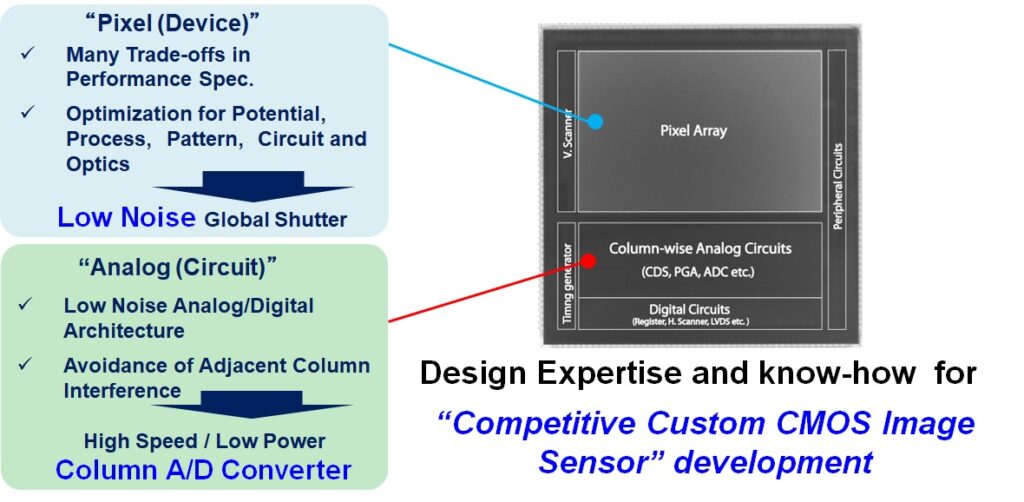
Technologies for Image Sensor Ⅱ
1) Pixel Design
★ Optimization by considering many Trade-offs
★ Global Shutter
★ Time of Flight
→Customize Pixel with Foundry
2) Analog Design
★ Low noise Amplifier
★ High Speed ADC(A/D Converter) = Cyclic ADC
Cf. Sony/OVT : Single Slope ADC
Aptina : SAR ADC
Technologies for Image Sensor Ⅲ
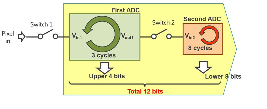
2-stage Column Parallel Cyclic A/D Converter
・Optimize the topology of the basic 2-stage Cyclic A/D Converter
・Brushed up the design for circuit and layout
High Speed (1MS/s)
High Bit Resolution (12bit)
Low Power (<120uW/ADC)
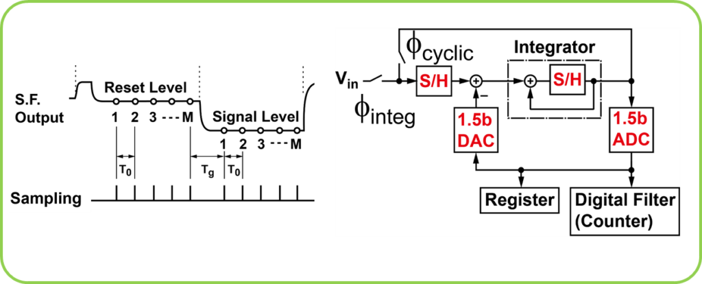
Correlated-Multiple-Sampling (CMS) 16b
A/D Converter
◆Our CMS-based cyclic ADC realizes ultra-low-noise wide-dynamic-range CMOS imagers for High-End DSC, Security Camera, Remote Sensing, etc.
Ultra Low Noise (0.3e-*)
High Bit Resolution (16bit)
Wide Dynamic Range (>90dB)
High Conversion Gain Pixel is used.
Technical Papers for Image Sensor
◆ 2017.02. ISSCC
“A 0.44e-rms Read-Noise 32fps 0.5Mpixel High-Sensitivity RG-Less- Pixel CMOS Image Sensor Using Bootstrapping Reset”
◆ 2016.02. ISSCC
“A 1.1μm 33Mpixel 240fps 3D-Stacked CMOS Image Sensor with 3-Stage Cyclic-Based Analog-to-Digital Converters”
◆ 2012.02. ISSCC
“A 33Mpixel 120fps CMOS Image Sensor Using 12b Column-Parallel Pipelined Cyclic ADCs”
◆ 2011.06. IISW
“A High Speed Low-Noise CIS with 12b 2-stage Pipeline Cyclic ADCs”
◆ 2011.06. IISW
“A 33Mpixel, 120fps CMOS Image Sensor for UDTV Application with Two-stage Column- Parallel Cyclic ADCs”
Technologies for Time of Flight Sensor I
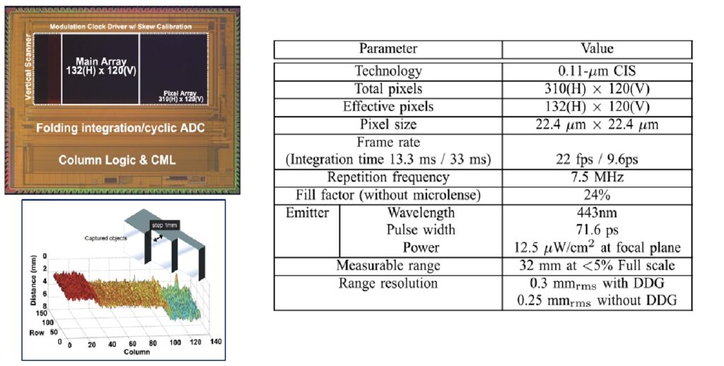
Technical Papers for Time of Flight Sensor
2015.05. J-EDS
“A Time-of-Flight Range Image Sensor with Background Cancelling Lock-in Pixels Based on Lateral Electric Field Charge Modulation”,
2016.01. Trans. on ED
“A Submillimeter Range Resolution Time-of-Flight Range Imager With Column-Wise Skew Calibration”
2016.01. Trans. on ED
“A 10 ps Time-Resolution CMOS Image Sensor With Two-Tap True-CDS Lock-In Pixels for Fluorescence Lifetime Imaging”
2014.08. Opt. Express
“Indirect time-of-flight measurement technique with impulse photocurrent response for sub- millimeter range resolved imaging”
2016.02. Opt. Express
“Single-event transient imaging with an ultra-high-speed temporally compressive multi-aperture CMOS image sensor”
Evaluation and Analysis Technologies
We can provide your pixels characterization data as well as haracterization environment and method and also FA data and method w/ OBRICH, SEM and TEM based on our rich experience.
Design Experiences on Large field image sensor
- Our strong point is Large format image sensor developments w/ special purpose.
- We have developed more than 15 large field image sensors w/ stitching on 0.11um CIS process in some foundry
- We have an Foundry expert who worked for some foundry for 15 year at technical support for Japanese customers on various processes include CIS processes.
◆Flexible image sensor design is available on a Large field image sensor
- Consideration for IR drop on bus lines.
- Keep clock simultaneity on a chip everywhere.
- Adjust many of High speed outputs data timing.
- Control Pixels behavior at stitching area.
- Ideas and experiences for large-field chip cost down and yield improvement.
- Test program development is available by ourselves, we can use Shizuoka univ. testers for image sensor.
- Failure analysis and short and log term reliability testing are also available.
